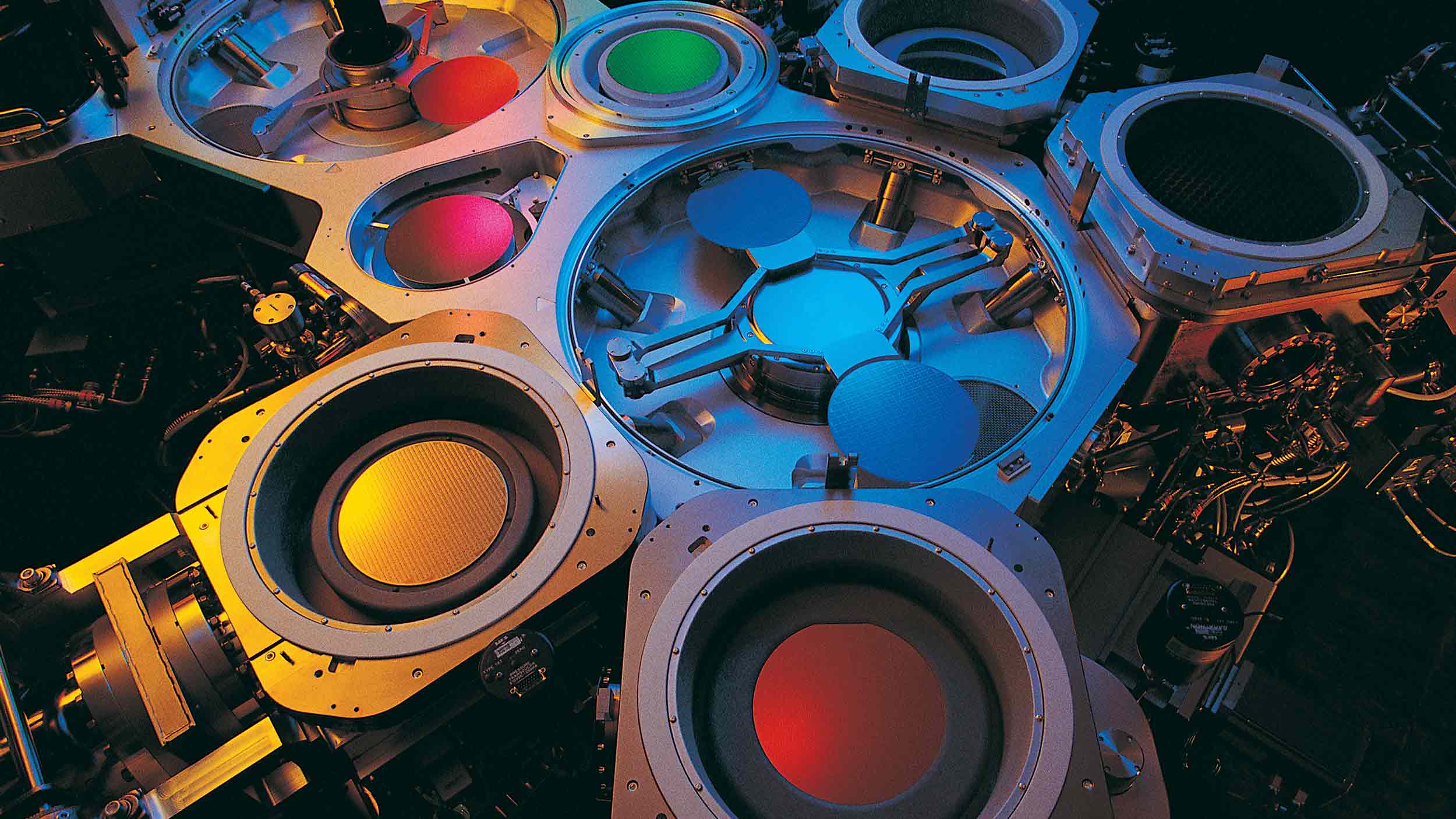
Following the polishing process, the wafers are etched with their respective circuitry layouts prior to going through the chemical vapor deposition (CVD) process. Here, the wafer is placed in a gas chamber and is continuously heated in various ways, depending on the facility.
As the gaseous reactant is being baked onto the wafer surface, temperature is critical to the final product of the wafer. During this process, a fixed sensor can be placed outside of the gas chamber to continuously take the temperature of the wafer – ensuring nothing damages the wafer.


